Recently study researchers used ultrafast electron microscopy to look directly at the coupling between gold nanoparticles and graphene.

Everyone who has ever been to the Grand Canyon can relate to having strong feelings from being close to one of nature’s edges. Similarly, scientists at the U.S. Department of Energy’s (DOE) Argonne National Laboratory have discovered that nanoparticles of gold act unusually when close to the edge of a one-atom thick sheet of carbon, called graphene. This could have big implications for the development of new sensors and quantum devices.
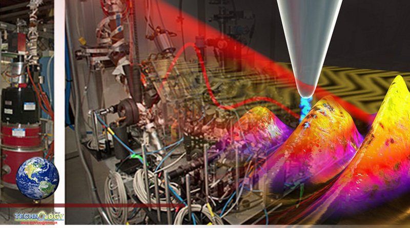
This discovery or technology was made possible with a newly established ultrafast electron microscope (UEM) at Argonne’s Center for Nanoscale Materials (CNM), a DOE Office of Science User Facility. The UEM enables the visualization and investigation of phenomena at the nanoscale and on time frames of less than a trillionth of a second. This discovery could make a splash in the growing field of plasmonic, which involves light striking a material surface and triggering waves of electrons, known as plasmonic fields.
For years, scientists have been pursuing development of plasmonic devices with a wide range of applications — from quantum information processing to optoelectronics (which combine light-based and electronic components) to sensors for biological and medical purposes. To do so, they couple two-dimensional materials with atomic-level thickness, such as graphene, with Nano sized metal particles. Understanding the combined plasmonic behavior of these two different types of materials requires understanding exactly how they are coupled.
“Surface plasmons are light-induced electron oscillations on the surface of a nanoparticle or at an interface of a nanoparticle and another material,” said Argonne non scientist Haihua Liu. “When we shine a light on the nanoparticle, it creates a short-lived plasmonic field. The pulsed electrons in our UEM interact with this short-lived field when the two overlap, and the electrons either gain or lose energy. Then, we collect those electrons that gain energy using an energy filter to map the plasmonic field distributions around the nanoparticle.”
In studying the gold nanoparticles, Liu and his colleagues discovered an unusual phenomenon. When the nanoparticle sat on a flat sheet of graphene, the plasmonic field was symmetric. But when the nanoparticle was positioned close to a graphene edge, the plasmonic field concentrated much more strongly near the edge region.
It’s a remarkable new way of thinking about how we can manipulate charge in the form of a plasmonic field and other phenomena using light at the nanoscale,” Liu said. “With ultrafast capabilities, there’s no telling what we might see as we tweak different materials and their properties.”
This whole experimental process, from the stimulation of the nanoparticle to the detection of the plasmonic field, occurs in less than a few hundred quadrillionths of a second.
“The CNM is unique in housing a UEM that is open for user access and capable of taking measurements with nanometer spatial resolution and sub-picosecond time resolution,” said CNM Director Like Arslan. “Having the ability to take measurements like this in such a short time window opens up the examination of a vast array of new phenomena in non-equilibrium states that we haven’t had the ability to probe before. We are excited to provide this capability to the international user community.”
The understanding gained with regard to the coupling mechanism of this nanoparticle-graphene system should be key to the future development of exciting new plasmonic devices.
Source Technology Networks